
Manufacturers and engineers in the electronics industry are constantly seeking advanced methods to ensure the reliability and safety of their products. Among these techniques, non-destructive x-ray stands out as a vital tool. This method allows for the in-depth examination of components without causing any damage. Providing invaluable insights into the quality of the connectivity and the internal workings of electronic devices.
In this blog post, we will explore non-destructive x-ray, its applications, and its indispensable role in the electronics industry, highlighting how it is key to the development of high-quality, durable electronics.
Understanding Non-Destructive X-RAY
At its core, non-destructive x-ray is a testing method that uses electromagnetic radiation to capture images of an object’s interior without altering or harming the item. Think of it as taking an X-ray of electronic components and assemblies to see inside without having to cut them open. This process is crucial for identifying manufacturing process faults, hidden flaws (for example ESD damage) or potential failure points in electronic assemblies and components, which are often hidden from sight or are too small to be detected by the naked eye.
The technique relies on the differential absorption of radiation by various materials. When x-rays pass through an object, denser materials absorb more radiation, resulting in darker areas on the radiographic image. Whereas less dense materials allow more radiation to pass through, appearing lighter. This contrast creates a detailed picture of the internal structure, revealing any irregularities or defects.
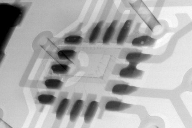
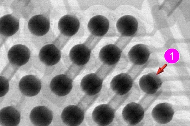
In the electronics industry, where precision is crucial, x-ray inspection offers a significant advantage. It enables the examination of solder joints, circuit boards, and other critical components (such as BGA’s and QFN’s) in a non-intrusive manner. Combine this with the expertise of our highly trained IPC Certified technicians and even the most minimal of defects can be found before products are mass produced or distributed for use in the field.
The Use of Non-Destructive X-RAY in Quality Assurance
Quality assurance is a vital aspect of the electronics manufacturing process. Where the goal is to deliver products that meet strict standards of reliability and performance. Non-destructive x-ray plays a crucial role in achieving this, by allowing for thorough inspection and analysis of electronic components throughout the production cycle. Including meeting the IPC standards of all class 1, 2 and 3 electronics.
By including x-ray as a standard step in the production process, manufacturers can detect issues such as soldering defects (for example voiding), component misalignments, FOD, bridging, short circuits and structural weaknesses before the final assembly stage. This proactive approach to quality control not only minimizes the risk of product failures but also contributes to the optimisation of manufacturing processes, leading to improved efficiency and reduced waste.
Using our state-of-the-art x-ray machine, our IPC certified technicians can provide accurate and reliable inspections, detailed reports and expert consultations as part of the service we offer.
Applications of Non-Destructive X-RAY in the Electronics Industry
Non-destructive x-ray can be utilised in various stages of the electronics manufacturing process, from prototyping and fault finding to final quality control. One of the primary uses is in the inspection of printed circuit board assemblies (PCBAs), where it helps identify issues such as solder voids, bridged connections, dry joints, head in / on pillow faults, counterfeit chips, and component & layer misalignments. These defects, if left undetected, could lead to short circuits, overheating, intermittent or complete failure of the electronic device, which in some cases can be fatal.
In addition to PCBs, this method is also used for assessing the integrity of semiconductor packages and integrated circuits. As electronic components become increasingly miniaturized, the demand for precise and reliable inspection techniques grows. Non-destructive x-ray can be used to ensure they meet the required specifications.
Furthermore, the technique supports the development of new products by allowing engineers to examine prototypes in great detail. This capability accelerates the design process, as it enables quick identification and correction of design flaws without the need for destructive testing.
While Non-destructive x-ray inspection is primarily used for the inspection of Surface mount components and assemblies, there is a very important role for it in conventional / Plated Through Hole (PTH) inspection. It is the only Non-destructive method to inspect the solder fill in a through hole joint, something that is vital for the performance of the electronic assembly as well as determining if the solder joints meet the required IPC standard (class 1, 2 or 3).
The Impact of Non-Destructive X-RAY on Product Development
In the fast-paced world of electronics, the ability to quickly bring new products to market is a key competitive advantage. Non-destructive x-ray significantly contributes to this by facilitating rapid prototyping and testing. By providing immediate feedback on the assembly process, internal structure and integrity of prototypes, this method allows for swift iterations and improvements, speeding up the development cycle.
Importantly, the insights gained from non-destructive x-ray help in optimising designs for manufacturability. Engineers can use the detailed internal images and expert advice from our technicians to refine component placement and soldering techniques, ensuring that the final product is not only functional but also cost-effective to produce.
Advancements in Non-Destructive X-RAY Technology and Our New Machine
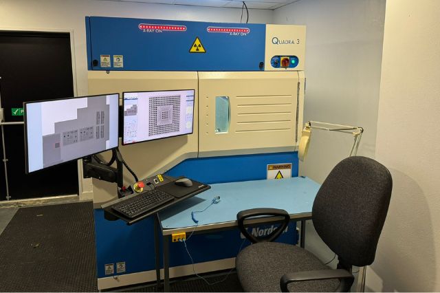
The field of non-destructive x-ray has seen significant advancements in recent years, driven by the needs of the electronics industry for more accurate and efficient inspection methods. The more modern x-ray machines, for instance, offer higher resolution images, the ability to conduct real time inspections from multiple angles and faster processing times compared to traditional film-based radiography. This improvement enhances the ability to detect even the smallest defects with greater precision.
The x-ray machine we have at our training center in Leeds is only a year old and far superior to the previous versions. It allows our technicians to produce instant images and assess components in even greater detail. We can offer the following specifications;
- < 0.95μm (950nm) Feature Recognition up to 10W Tube Power
- 160 kV Tube with Up to 10 W Tube Power – Always Retains Sub-Micron Ability
- Nordson DAGE AspireFP™3Mpixel @ 25fps with 50μm pixel pitch, Long Lifetime CMOS Flat Panel Detector Including Real Time Image Enhancements
- Geometric Magnification 2,000 X, Total 7,500 X
- 29″ x 22.8″ (736 x 580 mm) Maximum Board Size
- 70° Oblique Views Without Loss of Magnification
- AXiS – Active X-ray Image Stabilization
- High Quality Real Time Imaging
To find out more about the machine or how our team can assist in your production process and product assessment, get in touch with us today.
Non-Destructive X-RAY and Sustainability in Electronics Manufacturing
Sustainability has become a pressing concern in the electronics industry, with a growing emphasis on reducing waste and extending the lifecycle of products. Non-destructive x-ray contributes to these goals by enabling the early detection of defects and preventing the production of faulty items that would otherwise contribute to electronic waste.
By optimising manufacturing processes and reducing the need for rework, this technique helps conserve resources and energy. The detailed analysis provided by non-destructive x-ray also supports the development of more durable and reliable products, which in turn reduces the frequency of replacements and further contributes to sustainability efforts.
You can read more about the further benefits of x-ray testing in this article.
Why Work With Us
Here at EGL, we have supported the electronics industry for nearly 20 years with our non-destructive electronics testing.
While we are experts in electronics, we have also been known to provide x-ray services for other products when the need has arisen. If you have a product that needs internal and non-destructive inspection, then get in touch and see how we can work together to find a solution.
As technology continues to advance, we have no doubt that non-destructive x-ray inspection will undoubtedly continue to play a critical role in production and quality processes and help to shape the future of the electronics industry.
Get in touch today to find out more about how we can work together.